Most automated quality inspection technologies involve machine vision systems and, increasingly, aspects of artificial intelligence-powered software to speed the identification of part defects. But vision-based quality inspection is not the only quality inspection technology available to manufacturers. Another option is scanning acoustic microscopy (SAM).
Also known as ultrasonic non-destructive testing, SAM can identify small defects during manufacturing and analyze the specific root cause of a failure when a device fails in the field.
Hari Polu, president of Okos, a supplier of industrial SAM systems, says the SAM technology makes it possible for manufacturers to move to a higher level of failure analysis because of SAM’s ability to detect defects at a 50-micron level. “With this type of testing, we can inspect materials and discover flaws that were previously undetected,” Polu says.
He adds that a growing number of manufacturers are equipping their R&D and quality assurance labs with SAM, as well as integrating it into production lines for inspection. According to Polu, SAM testing is already the industry standard for inspection of semiconductor components to identify defects such as voids, cracks, and the delamination of different layers within microelectronic devices.
How SAM works
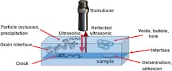
Using SAM, sound is directed from a transducer toward a small point on a target object. To produce an image for quality analyses based on the sound pulses, scans are produced. These scans range from single to multiple layers, which can include up to 50 independent layers. These multi-layer scans allow for “depth-specific information to be extracted and applied to create two-and three-dimensional images without the need for time-consuming tomographic scan procedures or X-ray equipment,” says Polu.
Polu says advanced, phased array SAM systems can detect minute flaws in specialty metals and alloys.
SAM at scale
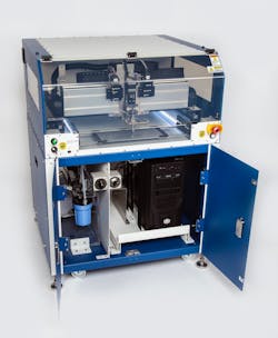
Even though small manufacturers can use a tabletop SAM system for scan envelopes of more than 300mm with a scan velocity up to 500 mm/s and accuracy and repeatability of +/- 5.0 micron, larger manufacturers typically require higher speed inspection capabilities.
Performing such high-speed inspections with 100% accuracy, as typically required by semiconductor manufacturers, requires automated equipment that can simultaneously inspect several layers, often on multiple channels.
“When high throughput is required for 100% inspection, ultra-fast single or dual gantry scanning systems are utilized along with 128 sensors for phased array scanning,” says Polu. “Multiple transducers can also be used to simultaneously scan for higher throughput.”
Polu noted that an advanced phased array with up to 128 sensors and accompanying software can enable inspection times of five minutes for granular detection of small impurities or defects, compared to the 45-minute inspection time required for a 5 MHz sensor to inspect an 8–10-in. square or disc alloy.
“Various software modes can be simple and user friendly, advanced for detailed analysis, or automated for production scanning,” says Polu. “An off-line analysis mode is also available for virtual scanning.”
Okos’ software-driven SAM model enables the company to reduce the costs of SAM testing while still delivering high quality inspection results, thus putting SAM technology “well within reach of even modest testing labs,” he says.
Leaders relevant to this article:


